Accurion UltraBAM


Accurion UltraBAM
-
Accurion UltraBAM
-
PARK SYSTEMS
-
Hàn Quốc
- Danh mục:
-
238
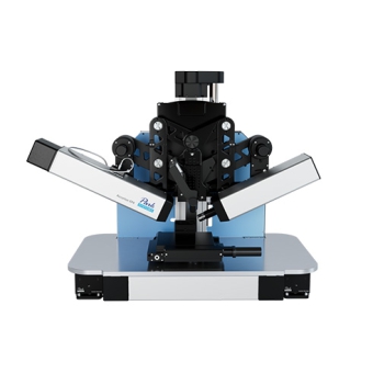
Accurion UltraBAM - The UltraBAM is the ultimate Brewster angle microscope designed for the air/liquid interface. It allows direct visualization of Langmuir monolayers or adsorbate films. It can also work on solid substrates like glass, quartz or similar materials.
- Giới thiệu
- Thông số kỹ thuật
- Ứng dụng và tiêu chuẩn
- video
- Tài liệu
Accurion UltraBAM
The UltraBAM is the ultimate Brewster angle microscope designed for the air/liquid interface. It allows direct visualization of Langmuir monolayers or adsorbate films. It can also work on solid substrates like glass, quartz or similar materials.*
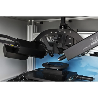
The UltraBAM combines high resolution and overall focused real-time imaging. Advanced imaging optics provide fully focused images at 20-35 frames per second. A high performance camera and specific calibration algorithms enable quantitative measurements of reflectivity. Thus, adsorption kinetics or thickness variations can be monitored. The instrument comes with a motorized analyser to visualize optical anisotropy caused by long-range molecular orientation order in monolayers.
The provided software makes operation easy and convenient. It allows taking pictures of the water surface with just one click or even automatize picture grabbing completely, so that the user only needs to concentrate on keeping the focus line in the live view. It is also possible to record videos for later analysis. Furthermore, the software provides image analysis tools like pixel count and automatic ROI selection for the evaluation of area coverage.
The UltraBAM and its software can be integrated with virtually any trough: on your existing trough**, or with one of our integrated troughs. The trough comes as a separate item and is not included as standard. The integration with the trough software works only in the way of taking some information from the trough and adding it as metadata to the pictures taken with the UltraBAM.
KEY FEATURES:
-
Spectroscopic imaging ellipsometry from 190/250/360 nm to 1000/1700 nm
-
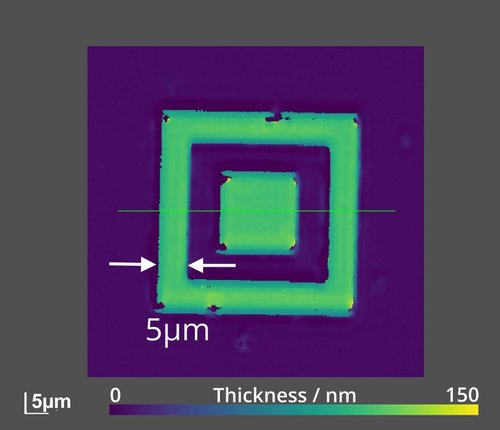
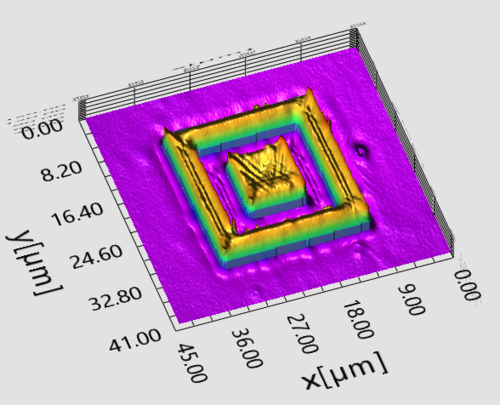
Highest lateral ellipsometric resolution of 1 µm, allowing to determine thickness (0.1 nm to 10 µm) and refractive index on microstructures as small as 1 µm
-
Ellipsometric enhanced contrast images for a live visualization of the sample
-
Intuitive selection of measurement region by drawing region in live view
-
Parallel measurement of multiple regions within the selected field of view
-
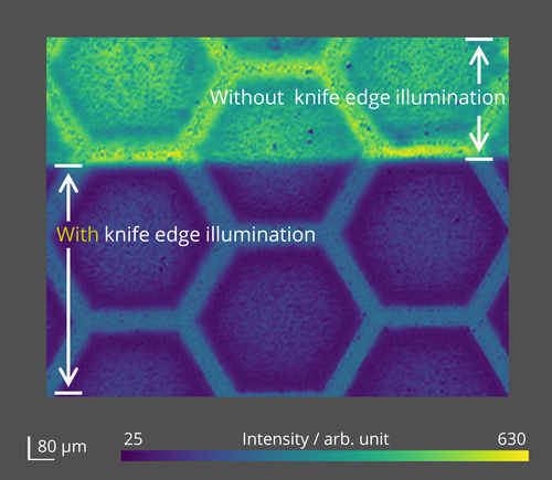
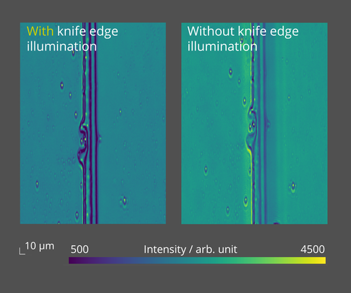
Patented knife-edge illumination for the non-destructive suppression of disturbing backside-reflections
-
Enlarge your measurement possibilities by using addition accessories, e.g. cells, temperature control or liquid handling
Technology:
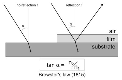
Brewster Angle Microscopy
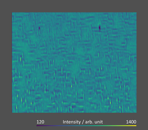
This microscopy technique allows the direct observation of ultrathin organic films on transparent dielectric substrates. It is based on the effect that from the clean surface no reflection occurs when p-polarized incoming light under the Brewster angle.
The "black background" of the Brewster angle setup allows using the detector (CCD-camera) with the maximum of intensity. A very thin organic layer (e.g. a monolayer with typ. 2 nm) with different refractive index will cause reflection. Typically, the resulting reflection is only about a millionth of the incident intensity.
The reflected light can be used to form a high contrast image of the lateral morphology of the layer, with applications in the life sciences and materials research.
APPLICATIONS
I. 2D-Materials
-
Spectroscopic ellipsometric measurements on flakes of 2D-materials with sizes down to 1µm
-
Microscopic maps of thickness distribution and refractive indices from 190-1700nm
-
Ellipsometric contrast micrographs (ECM) enable increased contrast imaging over e.g. optical microscopy to visualize layer numbers and inhomogeneities
-
Non-destructive measurements on transparent substrates using knife edge illumination to prevent unwanted backside reflections
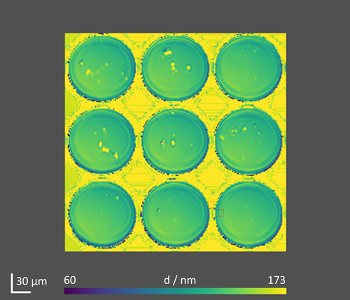
II. CURVED SURFACES
Ellipsometry is a very sensitive technique to measure thin films and antireflection (AR) coatings. However, it usually works for flat samples only. By using our patented technique in combination with the Imaging Ellipsometer ep4 on curved surfaces, we can overcome this issue and measure e.g. AR coatings on micro-lens-arrays.
-
Measure layer thickness and refractive index on curved surfaces
-
Investigate anti-reflection coatings on lenses, curved mirrors and micro-lens-arrays
-
Determine thickness distribution of multiple objects within a single measurement
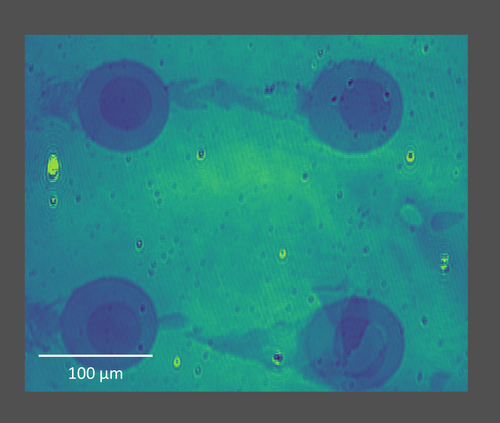
III. TRANSPARENT SUBSTRATES
Thin films on transparent substrates are of increased interest in advanced technologies like flexible displays, but this often raises the question of how to suppress disturbing backside reflections in a non-destructive manner. Knife edge illumination is a very effective tool to cope with this issue without damaging the sample.
IV. SURFACE ENGINEERING
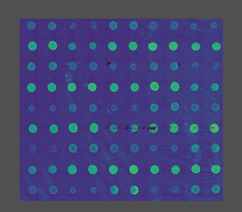
The main attempt of silanization is to form bonds across the interface between mineral/inorganic components and organic components present in paints, adhesives etc., or as the anchor for further steps of surface modifications.
This step proved to be difficult to measure with conventional methods. As for imaging ellipsometry, it provides the sensitivity to investigate e.g. the formation of bonds in a structured array for the use in micro-arrays without the need of an additional fluorescence marker, making it an exceptional device.
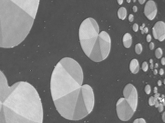
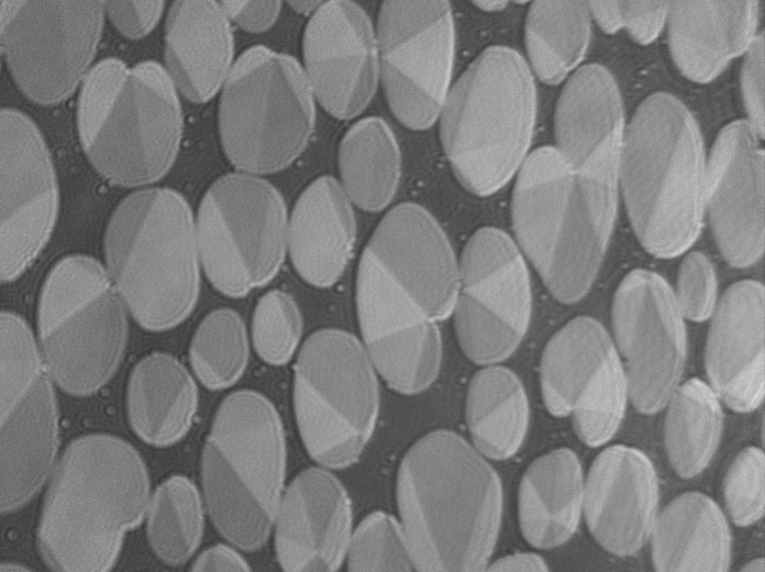
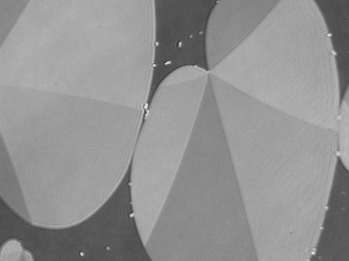
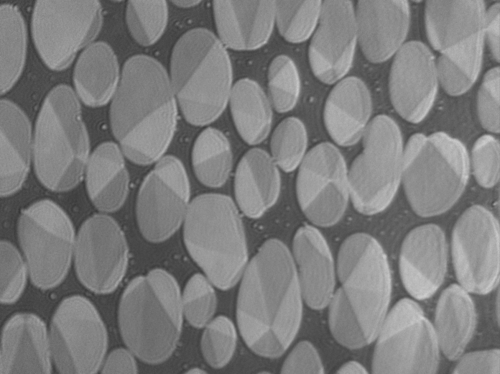
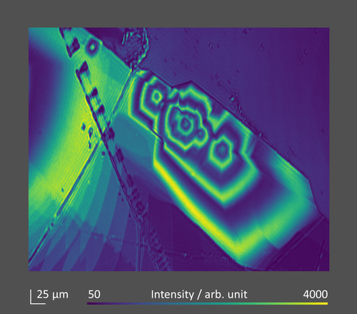
V. AIR-WATER INTERFACE
The air/water interface is of elementary interest in biophysics as well as in industrial applications. Brewster angle microscopy (BAM) is a powerful technique that allows for real-time visualization of Langmuir-Blodgett monolayers.
BAM applications visualize biological materials and systems, and enable the investigation of amphiphilic molecules, proteins, drugs, extracts, DNA, nanoparticles etc. at the air-water interface.
VI. ANISOTROPIC FILMS
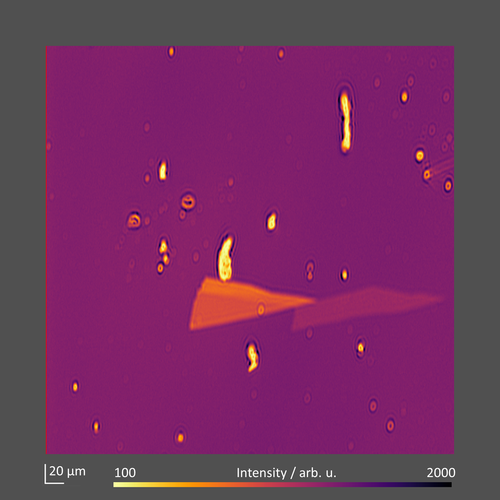
Anisotropic micro crystals show high potential for the applications in e.g. microelectronic devices and flexible electronics. Most organic single crystals indicate a highly anisotropic optical behavior. Regarding anisotropic samples, the refractive index depends on the polarization of light and direction of propagation.
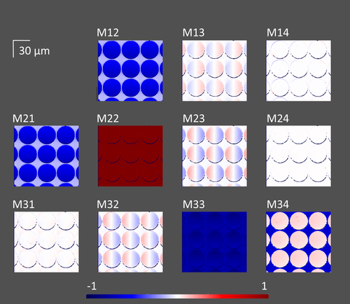
Imaging Mueller Matrix Ellipsometry (IMME) is an advanced technique required for the complete and accurate characterization of anisotropic and/or depolarizing samples. By using IMME with a microscope objective lens, the measurement of anisotropic refractive indices and the orientation of the optical axes becomes feasible even on micro-structured thin-film samples such as Black Phosphorous (BP) flakes.
VII. BIO-INTERFACES
Biological applications demand high sensitivity observation techniques. Additionally, the environment needs to be controllable in order to avoid influencing or damaging the behavior of observed materials.
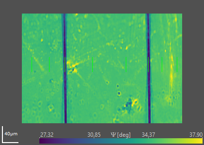
Imaging Ellipsometry (IE) offers highest sensitivity for thickness or surface coverage of mono- as well as sub-monolayers with microscopic resolution. High resolution micromaps of the ellipsometric angles Δ and Ψ, and the unique ellipsometric contrast mode for thin films offers insight in real-time to thickness changes on microstructures.
Useful accessories as e.g. cells, QCM-D etc. enlarge the field of measurement and research for biological applications.
Typical applications include:
-
In-situ Imaging Ellipsometry
-
Integration of QCM-D
-
Microscopic i-SPREE
-
Supported Bilayers
-
Biophysics
-
Microscopic Mapping
-
Microarrays / Microfilms
-
Biomolecular Interaction
VIII. MEMS
-
Spectroscopic ellipsometry on MEMS structures down to 1µm
-
Precise film thickness measurement on comb structure with 0.1nm thickness resolution
-
Multiple results from a single measurement: Film thickness, refractive index, composition, contaminations
-
ECM mode (Ellipsometric Contrast enhanced Microscopy) for fast quality control
-
Measurements on curved surfaces
Typical applications include:
-
MEMS sensors
-
MEMS mirrors and spring coating
-
RF MEMS
-
Thin film encapsulation
-
Gas analyzers
-
Humidity sensors
IX. PHOTONICS
-
Spectroscopic ellipsometry on small optical fibers and waveguides with lateral resolution down to 1µm
-
Precise refractive index measurement on waveguides, vertical facets and fiber ends with relative refractive index difference < 0.001
-
Precise film thickness measurement with 0.1nm thickness resolution
-
Wavelength range 190nm - 1700nm (IR upgrade to 2700nm possible)
-
Multiple results from a single measurement: Film thickness, refractive index, composition, contaminations
-
ECM mode (Ellipsometric Contrast enhanced Microscopy) for fast quality control
Typical applications include:
-
Photonics and waveguides
-
Integrated photonics
-
Vertical facets
-
Optical fibers
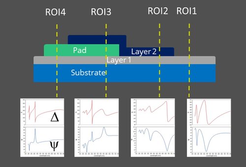
X. DISPLAYS
-
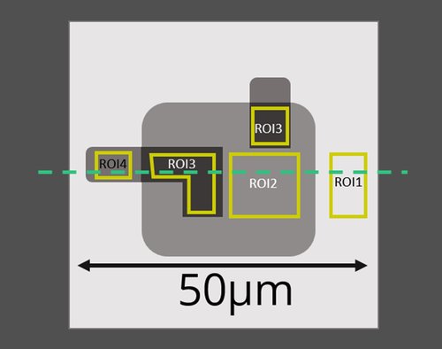
Spectroscopic measurements on few micron small regions, using patented ROI (Region Of Interest) concept
-
Each ROI (Region Of Interest) corresponds to another layer stack
⇒ Multiple measurements in a single run -
Coupling thicknesses between different models allows uncorrelating the results of multi layer films
-
UV wavelength range down to 190nm to characterize display materials
-
Multiple results from a single measurement: Thicknesses, optical dispersions, compositions
-
Pattented RCE6 mode allows tact times of < 20s
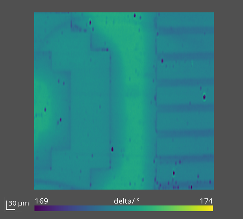
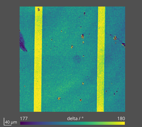
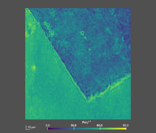
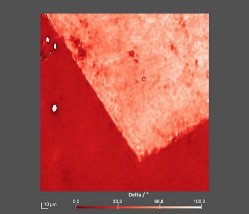
XI. BATTERY MATERIALS
-
To learn more about electrode materials for Battery applications, it is required to follow the charging/decharging of the system
-
A very promising approach is Operando Imaging Ellipsometry
-
Continuous measurements of Microscopic maps of Delta and Psi during charging and decharging of the sample
-
Extracting Delta and Psi from a large region of interest of the maps that represent the shape of the complete sample as well as from tiny regions of interest that represent only local properties of the film ⇒ Average and details from one measurement
-
Direct comparison of sample and substrate under exactly the same conditions
-
All analysis can be done in post process by having the complete maps recorded
-
Other processes like profiles, sub region analysis, histogram analysis, math functions etc. are available as well
Sản phẩm cùng loại
 Đọc thêm
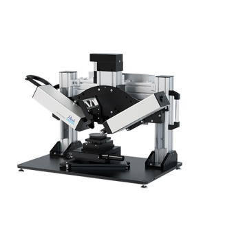


CÔNG TY TNHH THƯƠNG MẠI VÀ ĐẦU TƯ T&N
 Trụ sở: 19 Hàng Thiếc, P. Hàng Gai, Q. Hoàn Kiếm, TP. Hà Nội
Chi nhánh: 410/7A Cách Mạng Tháng 8, P.11, Q.3, TP. HCM
 Email: sales@tnic.com.vn/sale1@tnic.com.vn
 Hotline: HCM: 0905 653 866 | HN: 0982 028 728
 Website: tnic.com.vn
Copyright © 2020 CÔNG TY TNHH THƯƠNG MẠI VÀ ĐẦU TƯ T&N Designed by:Nina Co.,Ltd