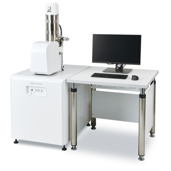
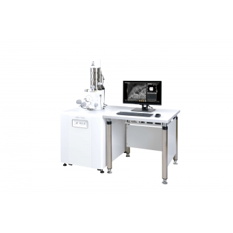
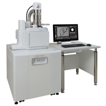
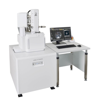
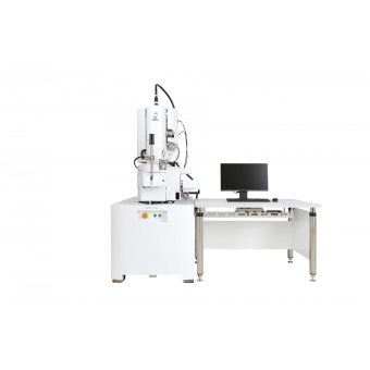
Kính hiển vi điện tử quét độ phân giải cao - JSM-IT710HR


Kính hiển vi điện tử quét độ phân giải cao - JSM-IT710HR
-
JSM-IT710HR
-
JEOL
-
Japan
- Danh mục:
-
321
- Giới thiệu
- Thông số kỹ thuật
- Ứng dụng và tiêu chuẩn
- video
- Tài liệu
Tính năng
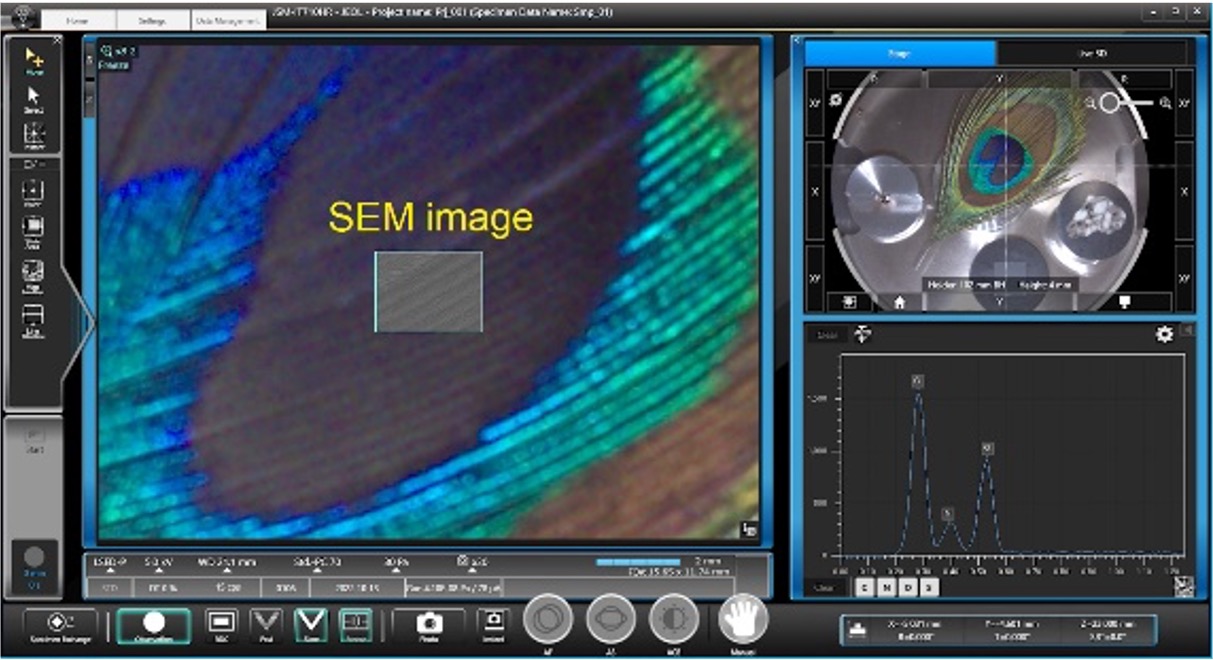
1. Hình ảnh SEM có thể được quan sát cùng với hình ảnh quang học
2. Hình ảnh được nhìn thấy rõ hơn nhờ súng điện tử có độ phân giải cao
Chức năng mới
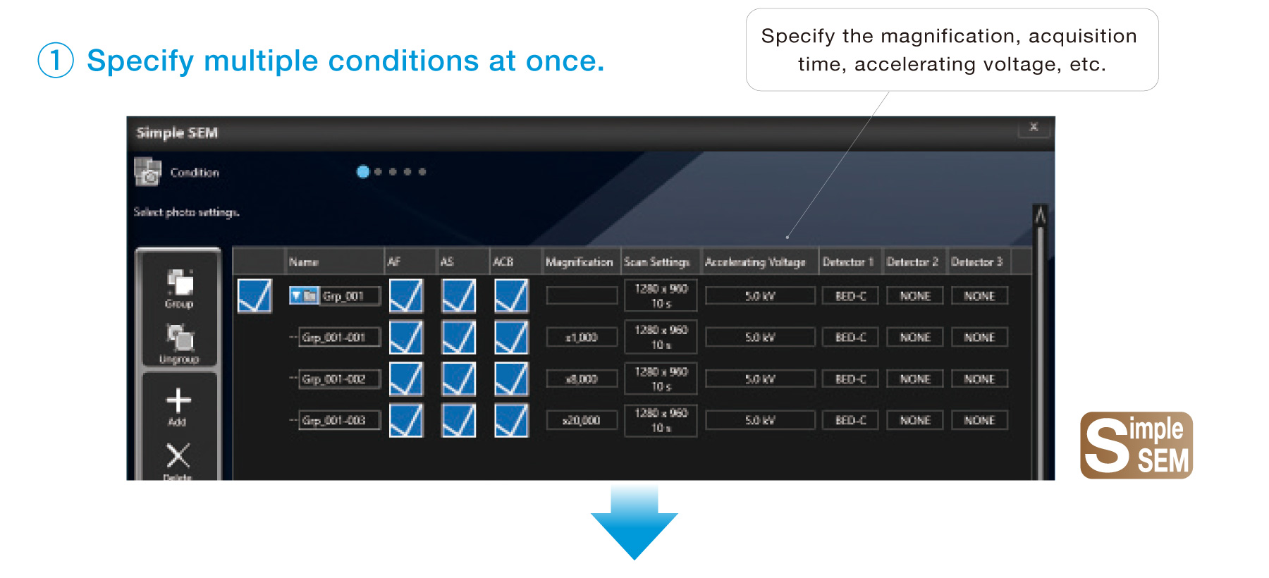
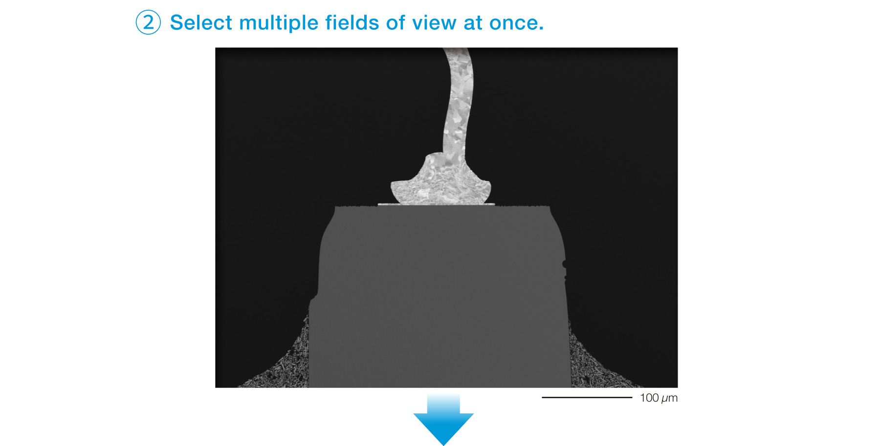
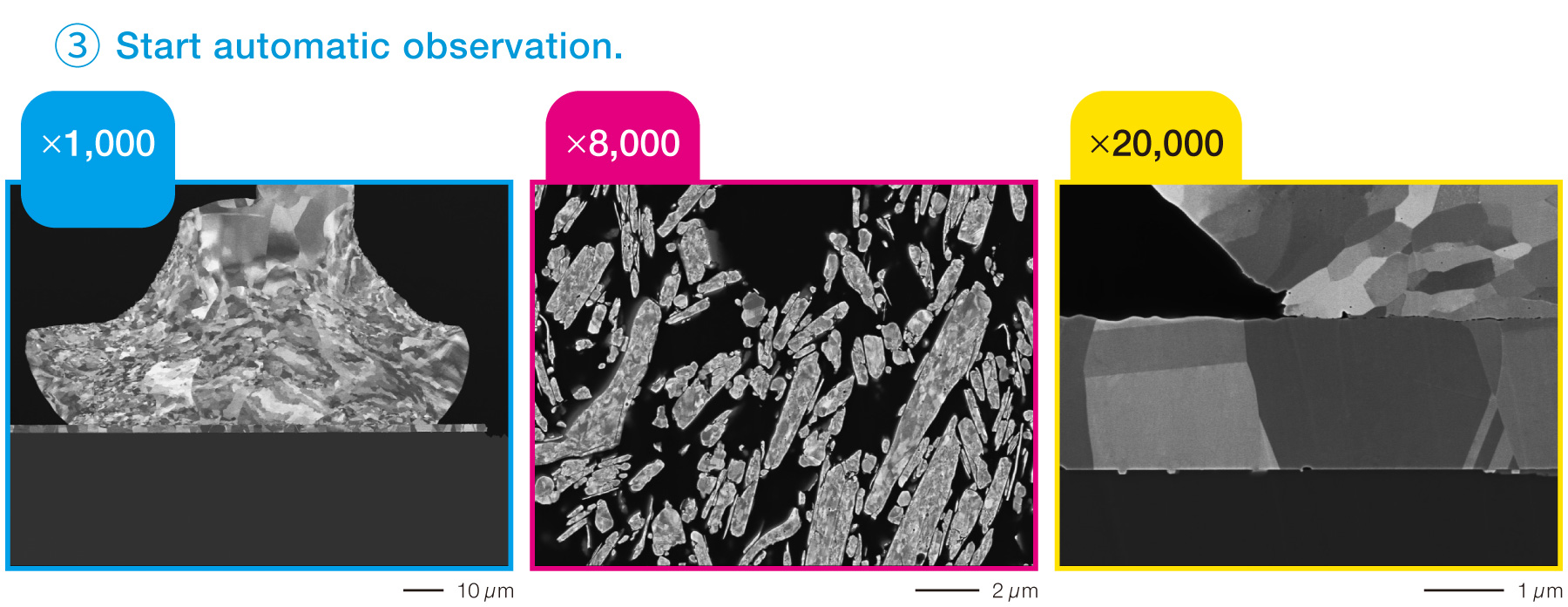
Chức năng quan sát tự động: Simple SEM/EDS
Simple SEM function enables automatic measurements by registering multiple conditions at once. Simple
This improves the efficiency of routine work.
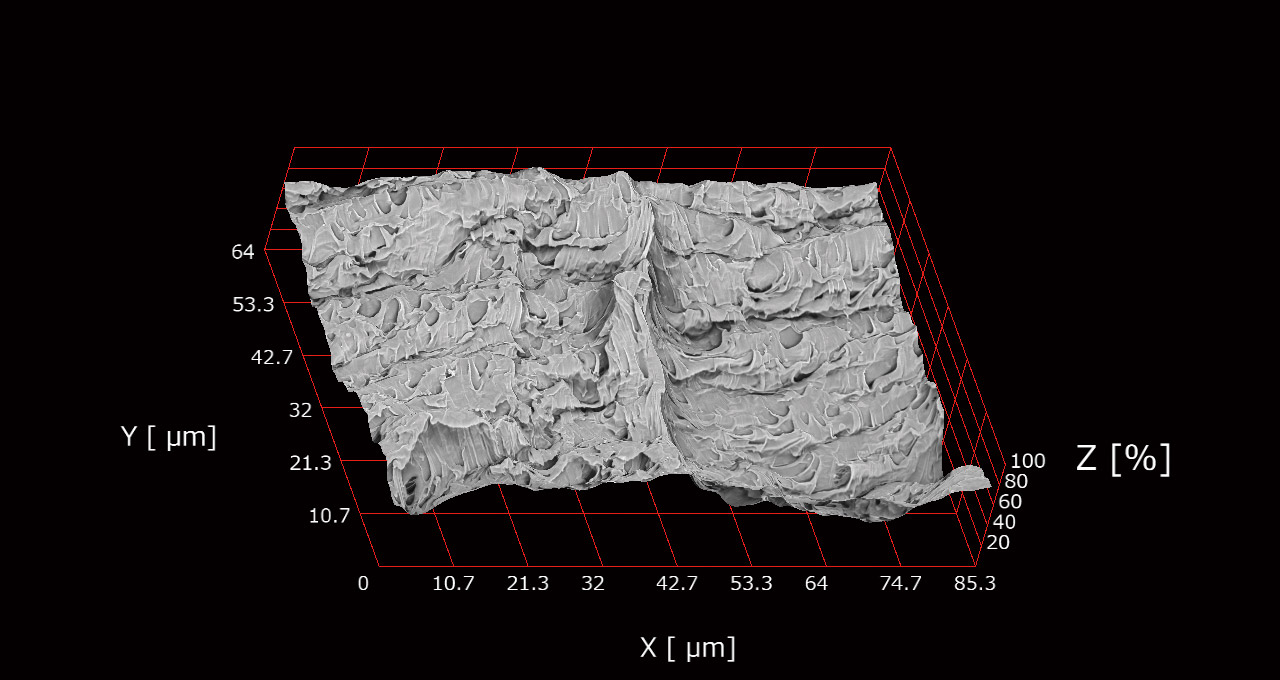
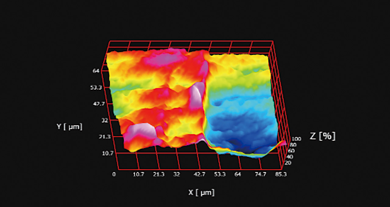
Live 3D: constructs 3D image on the spot
Imaging is possible at a low magnification with a little distortion, due to the out-lens objective lens.
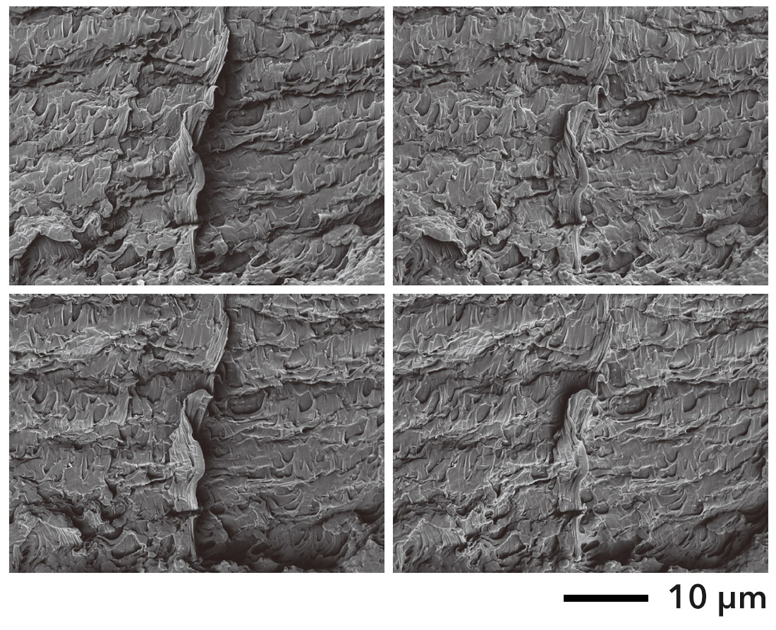
Live 3D image
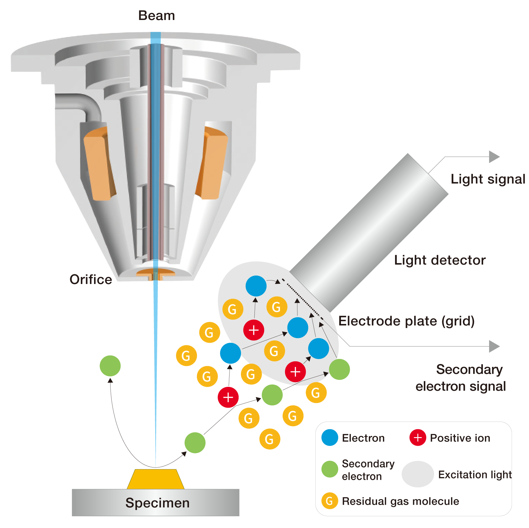
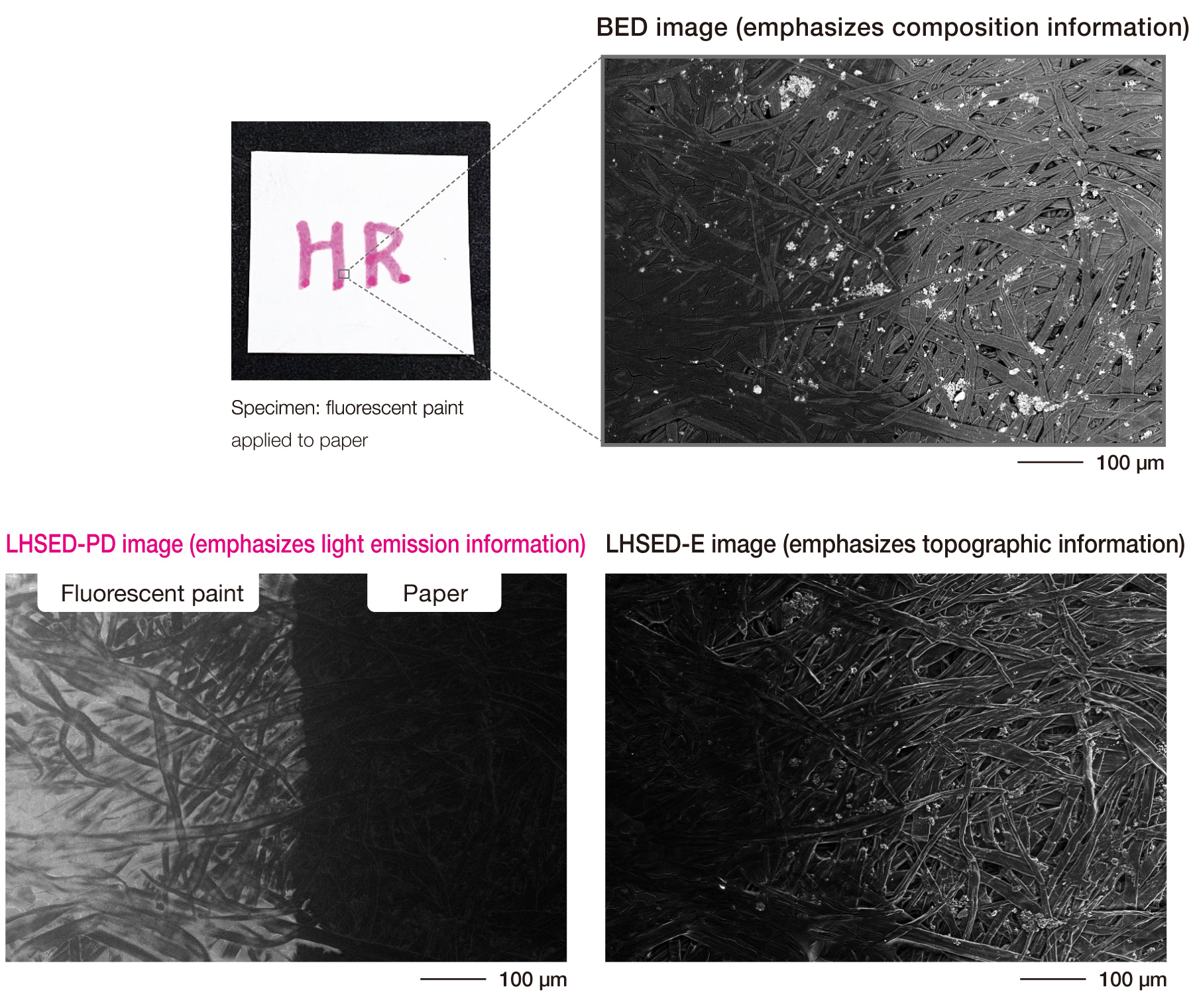
New Low Vacuum Hybrid Secondary Electron Detector (LHSE) ※Optional function
The LHSED, a new low-vacuum detector, enables observation while switching between images containing light emission information and topographic images.

LHSED Features
- Improved quality of low vacuum secondary electron live image
- Acquisition of light emission information
- Switching between topographic and light emission information image
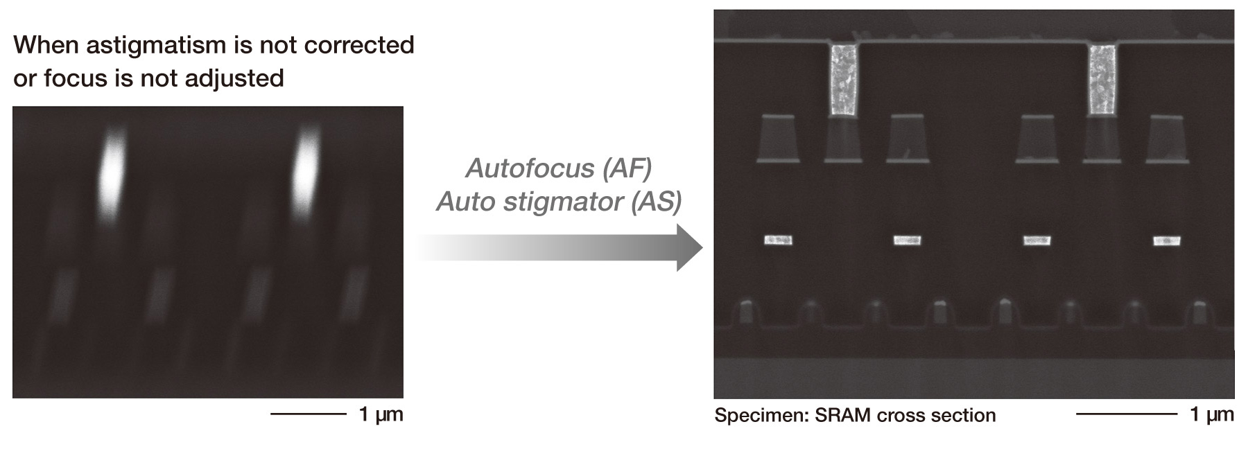
Schottky FE electron gun stability has been enhanced more than 4 times compared to the previous models
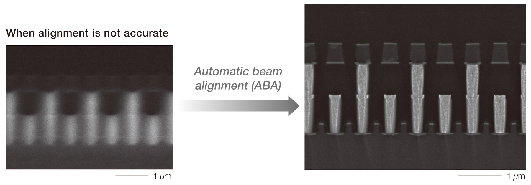
Automatic Beam Adjustment
JSM-IT710HR does not require complicated manual adjustment and provides automatic adjustment from axis alignment to astigmatism correction and focusing.
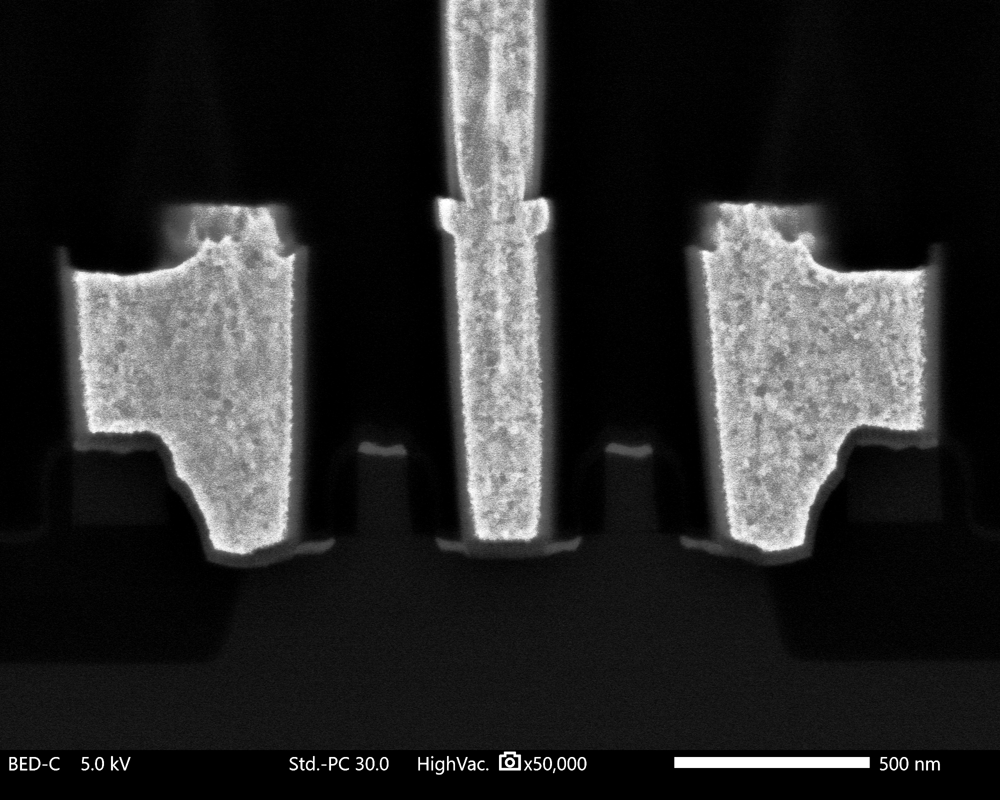
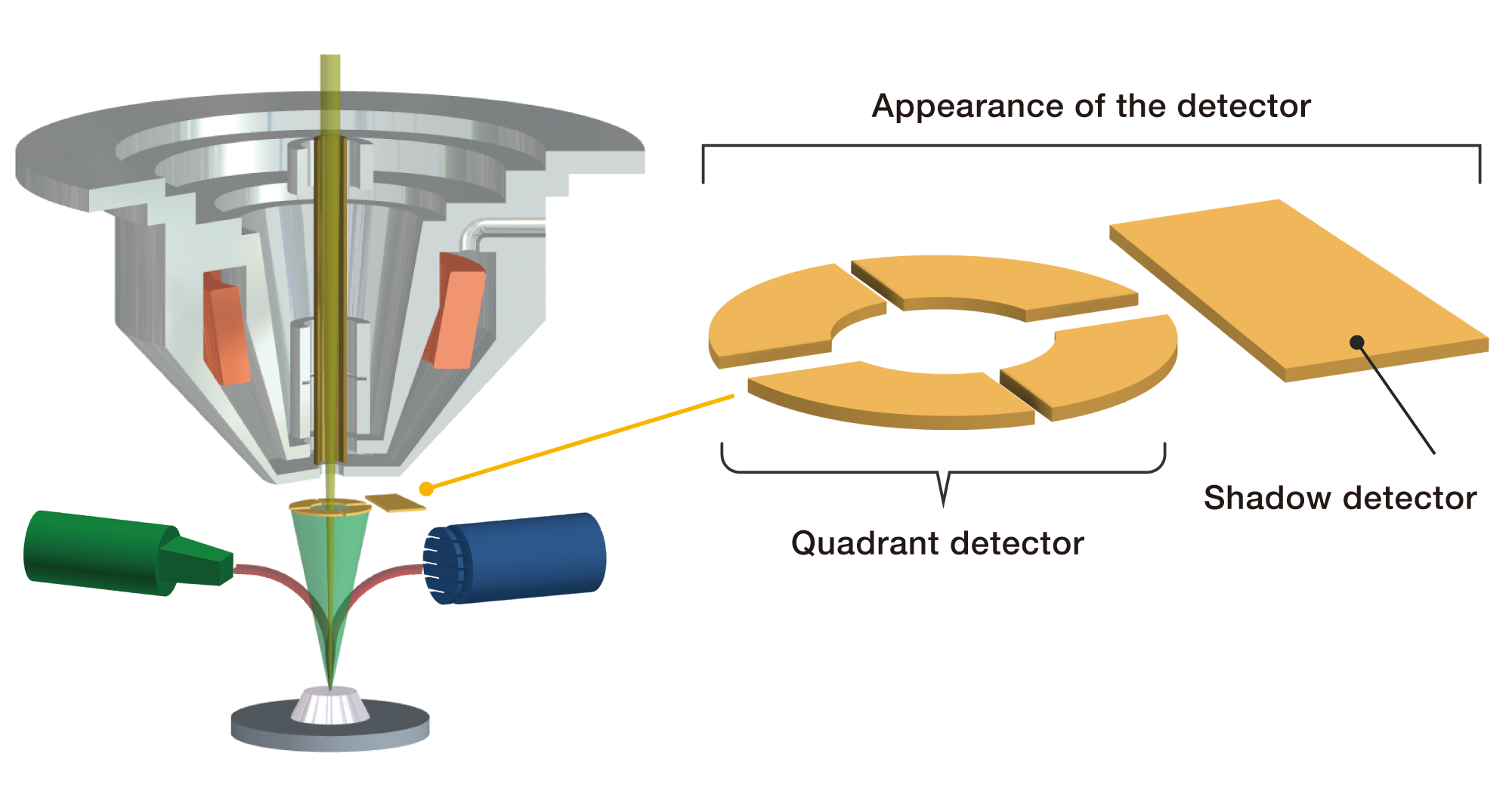
Secondary Electron Detection System
Secondary electron detector (SED)
 \
\
Low vacuum secondary electron detector (LVSED/LHSED)
Both High Resolution and Large Current
The Schottky field emission gun used in the JSM-IT710HR enables high-resolution observation and analysis because the electron gun is integrated with the condenser lens to create large currents while maintaining a small probe.
Backscattered Electron Detection System
The new multi-segmented backscattered electron detector acquires backscattered electron images from four directions at once so that a simple 3D image can be created and displayed live, in real-time.
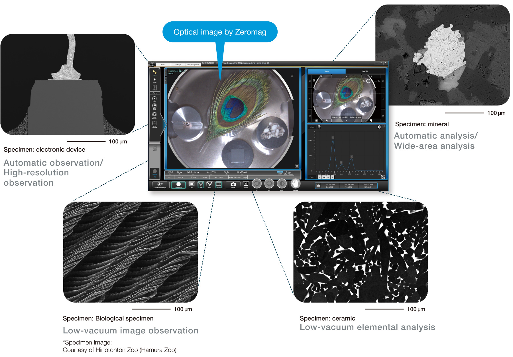
Every Analysis Starts with Zeromag
Zeromag's optical image simplifies navigation.
SEM images can be linked to optical images for easy observation, analysis, and automated measurements.
EDS Integration
JEOL manufactures and sells not only SEMs but also EDS.
Fully embedded EDS with SEM for simplified workflow, operation and data management.
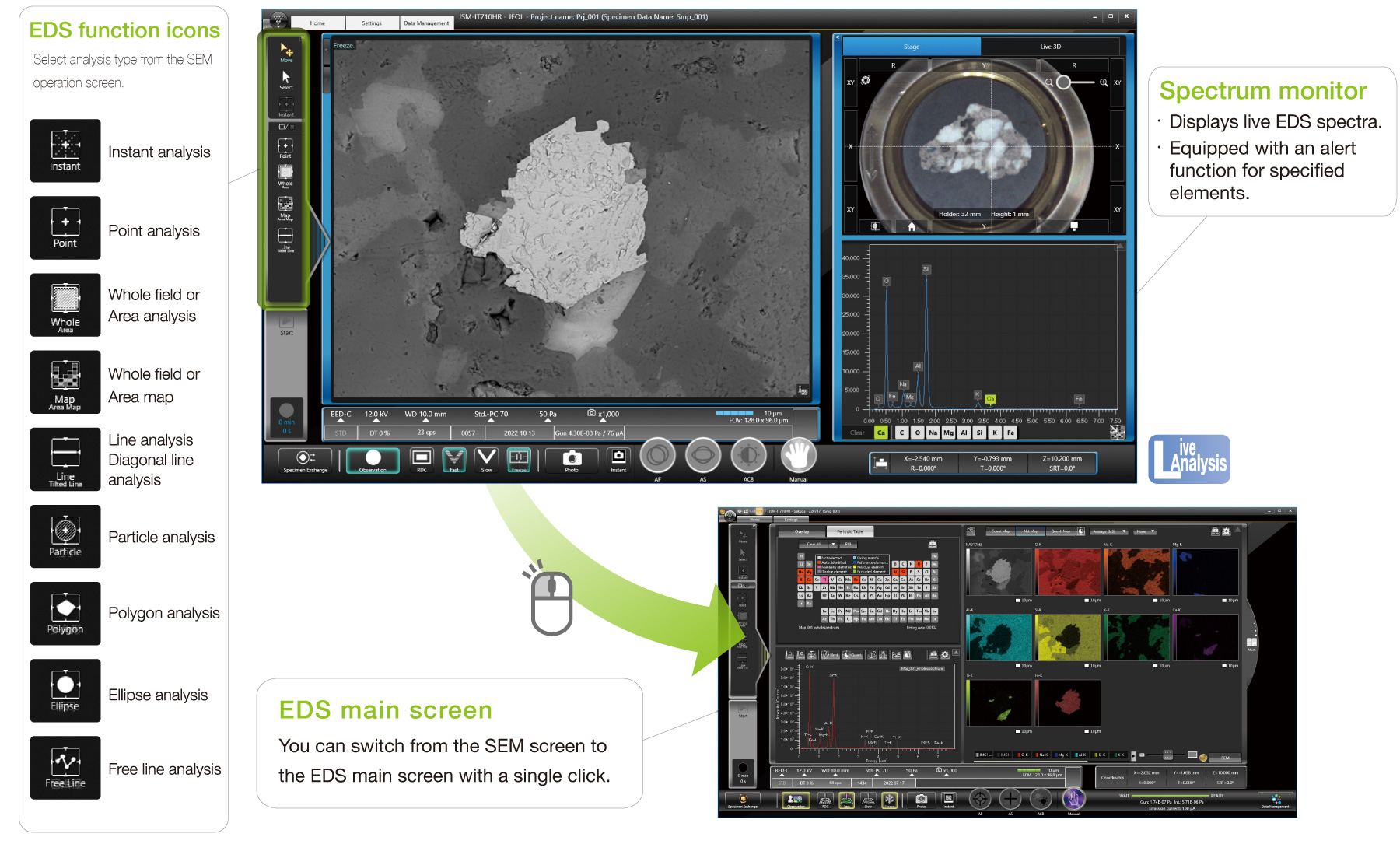
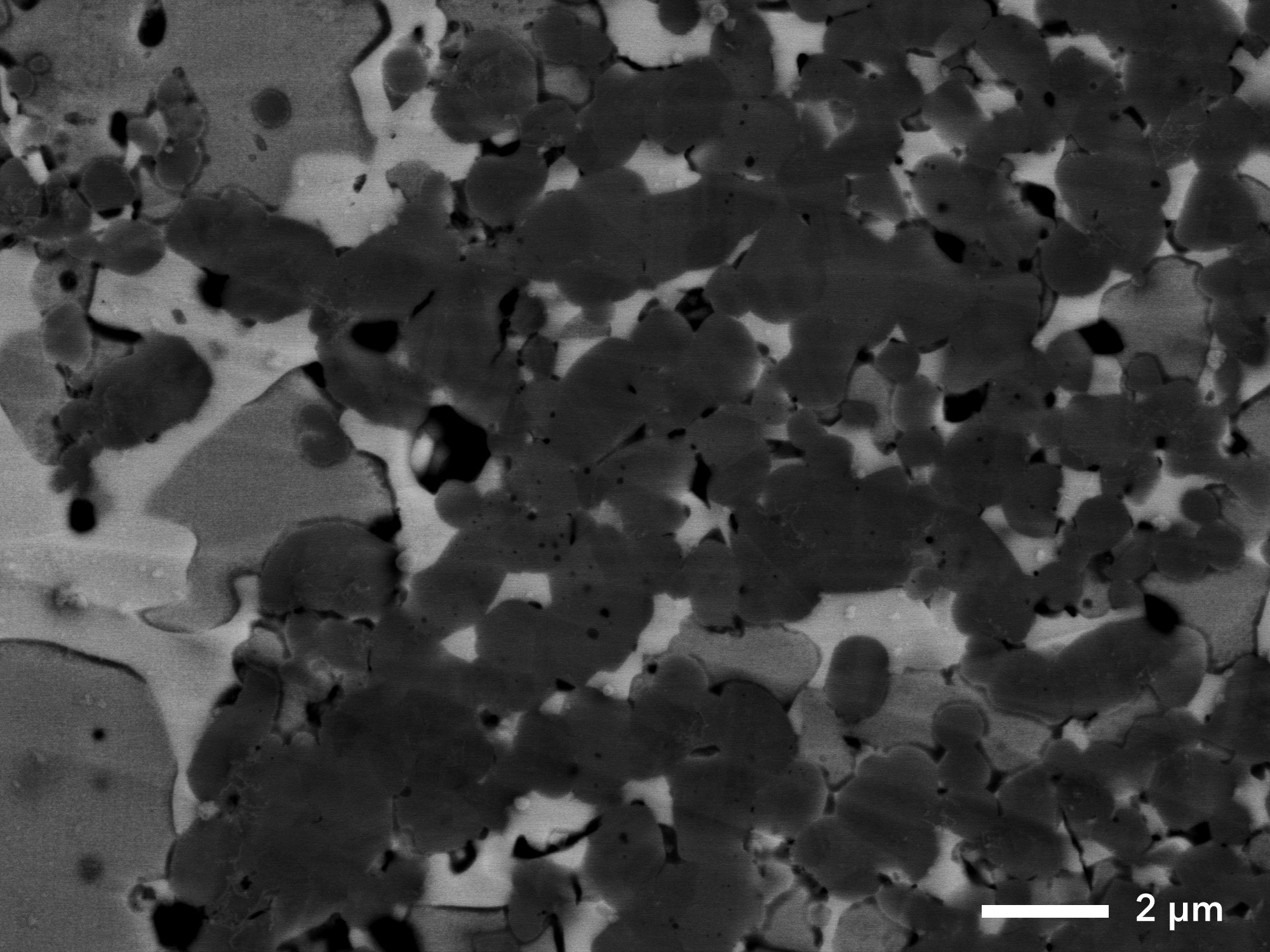
Phase Analysis
JEOL’s EDS system supports a new phase analysis function. Phase maps can be created from map data set.
Backscattered electron image
Phase mapping (Overlay of multiple phases)
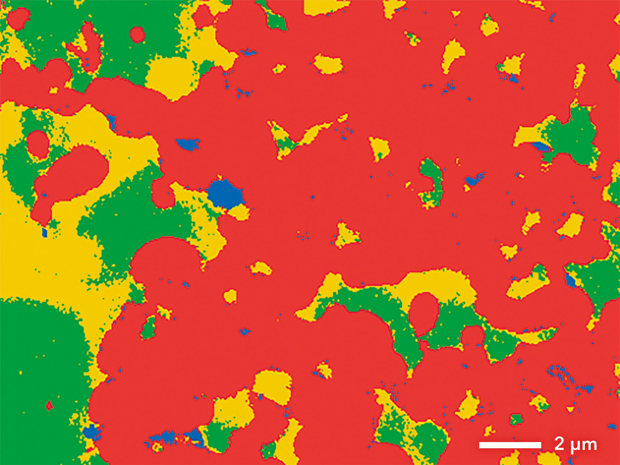
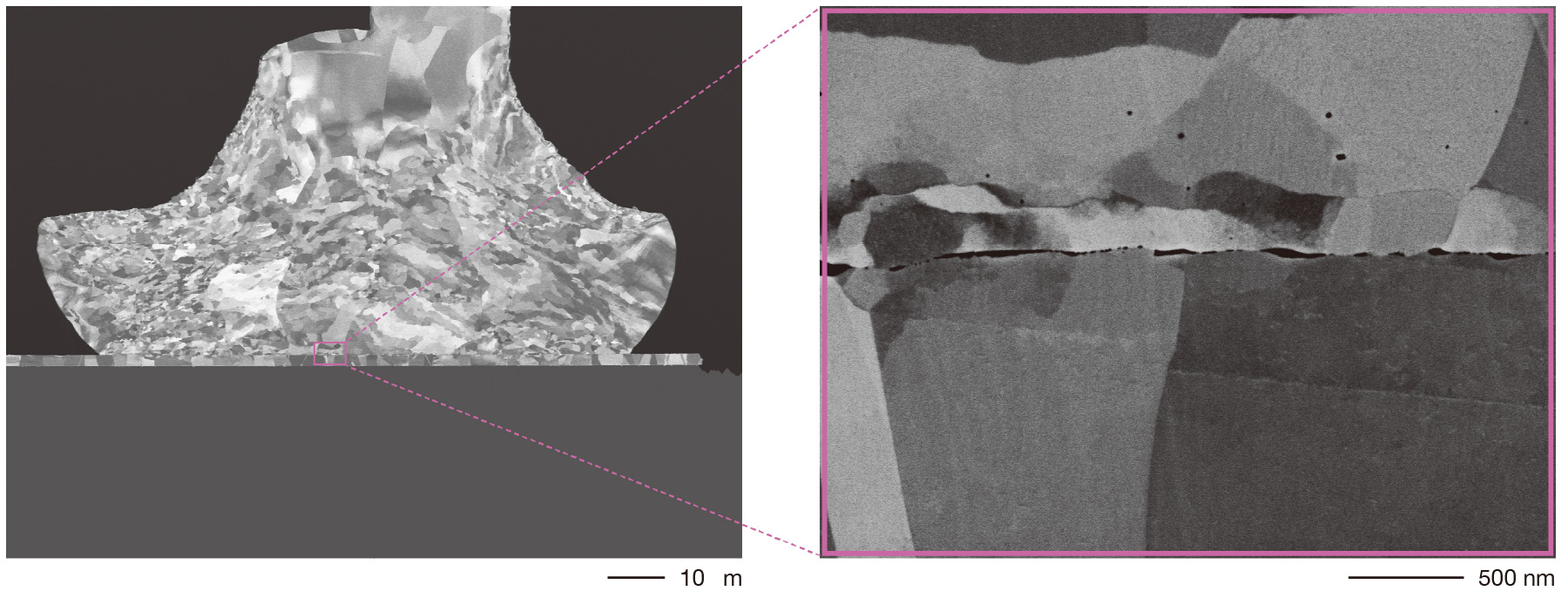
Specimen: cross section of a cutting tool for precision machining
Phase analysis indicates component difference between Co, Cu and Sn rich area
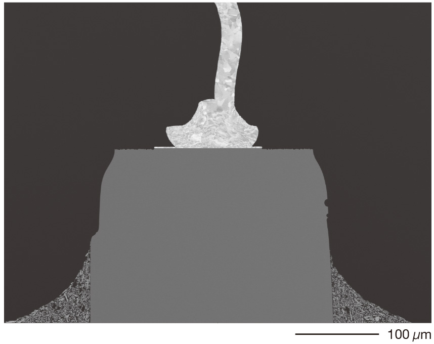
Electronic Devices
Applicable features of JSM-IT710HR: high r esolution, high contrast, wide-ar ea observation
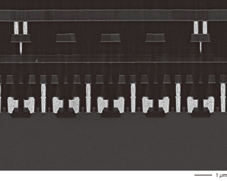
LED
Clear observation of a nanovoid at the junction interface of an electronic device
Specimen: LED cross section prepared using CP*
Magnification: ×250 (top), ×1,000 (bottom left), ×40,000 (bottom right)
Accelerating voltage: 5 kV
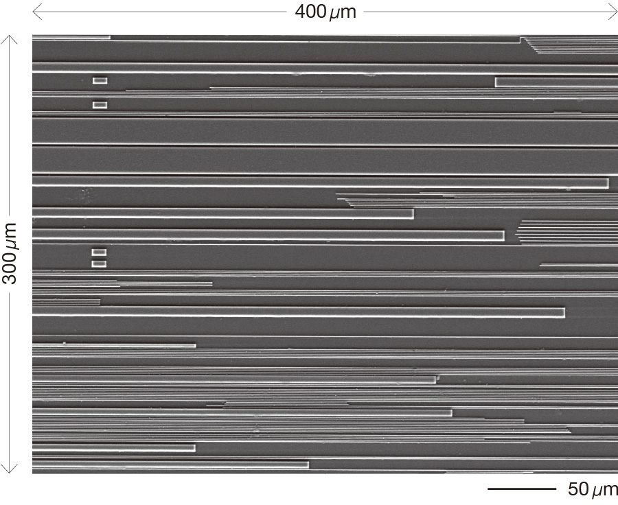
Wiring pattern
Using the low-vacuum function to observe a wide area of the wiring pattern surface
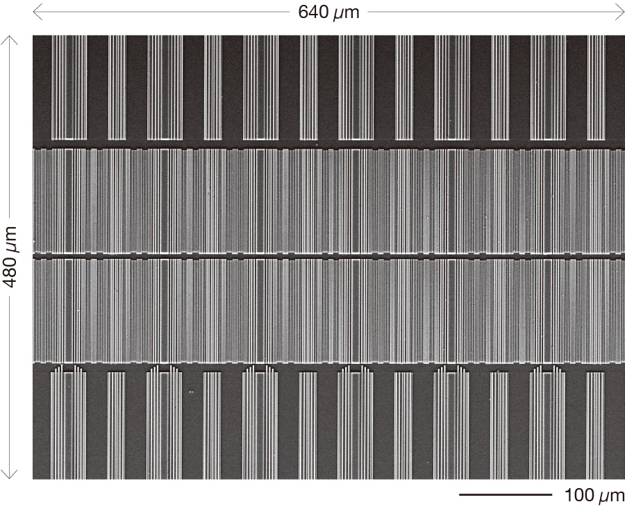
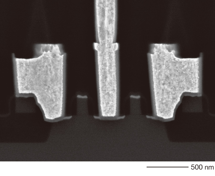
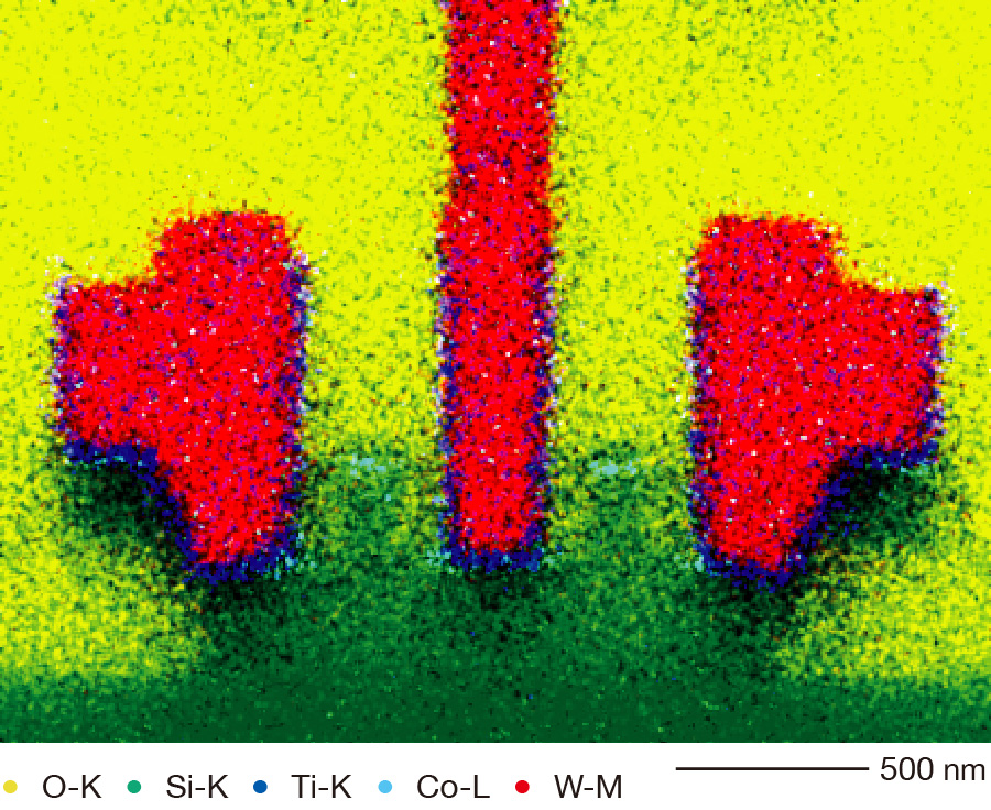
SRAM
High-resolution EDS map
Specimen: SRAM cross section prepared using CP
Magnification: ×10,000 (top), ×50,000 (bottom)
Accelerating voltage: 5 kV (SEM), 7 kV (EDS)
 Đọc thêm


CÔNG TY TNHH THƯƠNG MẠI VÀ ĐẦU TƯ T&N
 Trụ sở: 19 Hàng Thiếc, P. Hàng Gai, Q. Hoàn Kiếm, TP. Hà Nội
Chi nhánh: 410/7A Cách Mạng Tháng 8, P.11, Q.3, TP. HCM
 Email: sales@tnic.com.vn/sale1@tnic.com.vn
 Hotline: HCM: 0905 653 866 | HN: 0982 028 728
 Website: tnic.com.vn
Copyright © 2020 CÔNG TY TNHH THƯƠNG MẠI VÀ ĐẦU TƯ T&N Designed by:Nina Co.,Ltd